Earnings on Japan’s foreign direct investment (FDI) reached 103% of new FDI in 2022–25. With dividends and retained earnings counted together, Japan Inc. now needs to sell little yen to invest abroad.
[by OKUBO Takuji]
Key takeaways
- Foreign affiliates now earn about as much as Japan invests abroad each year. Reinvested earnings, dividends and interest together reached 103% of new outward FDI in 2022–25, against 48% in 1996–2000.
- Dividends from foreign affiliates account for a growing share of Japanese corporate profit. We estimate that foreign affiliates contributed 13.4% of Japan Inc.’s earnings in FY2025, up from 1.7% in FY1996.
- Corporate investment abroad now involves little net yen selling. After dividends and interest paid home, the estimated outflow has been close to zero since 2022, down from about ¥5 trillion a year, or about 1% of GDP, on average in the 2010s.
Japan’s FDI stock now earns 103% of new investment
It is often said that Japan’s ageing population and slow growth give its companies too few investment opportunities at home. A Japanese government report in 2024 included the following passages.
“Japan’s ageing and shrinking population depresses expected demand at home. Expected returns remain higher abroad, so Japanese companies have accelerated outward direct investment” (my translation). — MATSUBAYASHI Yōichi [松林 洋一], MOF PRI, chapter 8, p.136.
“Companies invested abroad because they saw no promising investments in Japan; they are unlikely to bring back every return. On a cash-flow basis, the external balance is in deficit and is one factor behind the weak yen” (my translation). — KARAKAMA Daisuke [唐鎌 大輔], MOF PRI, chapter 10, pp.178 and 175.
However, my review of recent data shows that while their premise of low growth prospects in Japan is probably still right, the direct investment Japan has accumulated abroad has reached a level where it earns enough to cover Japan’s new investment abroad. This changes the exchange-rate implication even if Japan keeps investing abroad.
As chart 1 shows, earnings on the accumulated investment stock rose from 48% of new outward FDI in 1996–2000 to 103% in 2022–25.
Chart 1
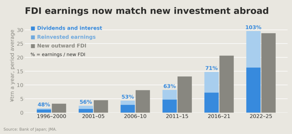
Overseas affiliates pay interest and dividends to their parent companies in Japan. Those dividends have become a sizable part of corporate Japan’s income: we estimate that they made up 13.4% of Japanese corporate profit in FY2025, up from 1.7% in FY1996.
When foreign affiliates retain their earnings on their balance sheets, Japan’s balance of payments statistics record them as FDI from Japan, even though no money crosses the border. While the companies receiving FDI dividends and the companies paying for new FDI are not necessarily the same, Japan Inc. as a whole is now financing its FDI almost entirely from the earnings of its overseas affiliates. At the current level of FDI, little new yen needs to be converted into foreign currencies as Japan goes about investing abroad.
In the rest of this report, I explain how foreign direct investment by Japanese companies evolved, and its near-term outlook. This report is the third in a series on the yen repatriation theme that I have published over the past few weeks, following “Yen Repatriation Starts with the Whale”, on capital flows through Japan’s national pension funds, and “Mrs Watanabe No More”, on Japanese households’ assets invested abroad.
A strong yen helped drive Japan’s first outward FDI boom
Japan’s outward investment was heavily restricted after WWII, requiring case-by-case permission from the government. Approvals became more and more automatic over the years until outward investment became “free in principle” in 1980. Trade friction with the US-led Japanese carmakers to restrain their exports from 1981, pushing them to build factories abroad. The rapid appreciation of the yen was also a factor. The yen strengthened from ¥242 per dollar before the Plaza Accord in September 1985 to ¥121 by the end of 1987. Japanese producers had to move lower value-added work abroad. The strong yen also gave Japanese financial institutions sizable purchasing power for a while, until the stock and property bubbles burst in 1990 and 1991.
All of these factors contributed to a rapid increase in outward FDI through the 1980s and 1990s (chart 2).
Chart 2

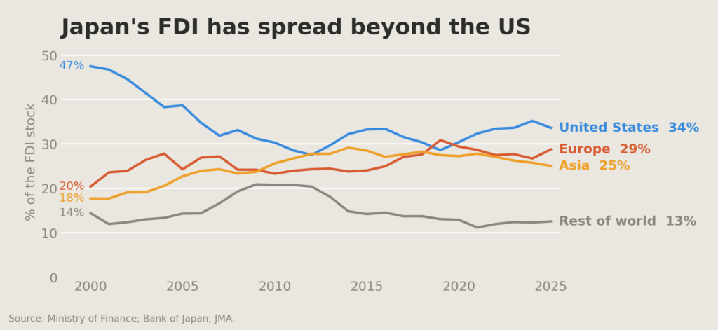
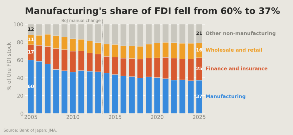
Even after the bubble burst, the strong yen kept pushing manufacturers to move abroad. In 2005, manufacturers accounted for 60% of the FDI stock. As Japanese manufacturers expanded their supply chains abroad, Asia’s share of outward FDI rose from about 12% in FY1986–90 to 19% in FY1995–99, and Asia held 23% of the FDI stock by 2005 (chart 3).
Chart 3
Japan’s outward FDI stock rose to 56% of GDP
The next phase was sustained by a different pressure. With weak growth and low interest rates at home, Japan Inc. kept investing abroad, across a broader range of industries. Between 1995 and 2025, the stock of FDI rose from 9% of Japan’s GDP to 58% (chart 4). In 2025, it is as large as about 38% of the private sector’s domestic fixed capital, on our estimate.
Chart 4

By industry composition and by destination compositions changed over time. Manufacturing’s share of the FDI stock had fallen to 37% by 2025, giving Japan’s FDI more breadth. By destination, we are seeing a revival of FDI toward the United States. It accounted for 34% of the stock in 2025, Europe 29% and Asia 25% (see earlier chart 3).
Thus, after decades of overseas investment, Japan’s FDI stock is now large enough that its earnings are sufficient to finance new investment abroad, at least for now. In the next section, I consider whether this will continue, and in particular whether Japanese companies may bring an even larger share of their overseas earnings back to Japan, given the weak yen, higher borrowing costs in yen and possibly better investment opportunities at home.
The weak yen has slowed offshoring, not reversed it
The real depreciation of the yen over the past 15 years made production in Japan more competitive. There is some evidence that manufacturers are considering bringing production back to Japan. The 2023 manufacturing white paper found more firms shifting production back from China than moving there, and they named the weak yen as one reason. We see some signs of reshoring. Japanese manufacturers’ overseas production ratio rose from 18.0% in FY2011 to 27.2% in FY2023, but it may have started to decline or at least stabilize. The ratio fell to 26.7% in FY2024. A Cabinet Office survey of listed manufacturers puts the ratio at 24.5% in FY2025, and their plan for FY2030 is broadly unchanged at 24.7%. The weak yen seems to have stabilized the wave of offshoring, but I see no firm evidence of a move back onshore yet.
Domestic investment has grown slowly despite the weak yen
There are tentative signs that domestic capital spending is starting to grow again. For three decades it grew at a very low speed. In real terms, private business investment rose only 26% between FY1997 and FY2025, less than 1% a year. In comparison, capital spending grew by about 4% a year on average in the United States. In my view, a weak currency is only one of the factors manufacturers weigh in designing their global production chains. The weak yen makes production in Japan competitive today, but they have also seen the exchange rate swing violently within short periods. Japan also has a shrinking population problem. It started to address it by opening a door to immigration, but the door is only tentatively open. Overall, my view is that the weak yen alone is unlikely to give Japan Inc. sufficient incentive to bring its capital back to Japan and to the yen.
Economic security is bringing some production home
The government is pushing harder than the currency, mostly in the name of economic security, even before the Takaichi government came along. The government currently has a ¥250 trillion domestic investment target for FY2040 and named AI and semiconductors among its 17 strategic fields. Semiconductors are where the money has gone furthest. In November 2024, under the Ishiba government, Japan committed more than ¥10 trillion of public support to AI and semiconductors by FY2030, aiming to draw more than ¥50 trillion of public and private investment over ten years. Japan managed to lure a TSMC plant to Japan, backed by a sizable subsidy. Rapidus, a government-supported Japanese semiconductor maker, has received a sizable subsidy and is building a factory in Hokkaido. Japan’s production of integrated circuits and discrete semiconductors rose from ¥2.7 trillion in 2019 to ¥4.1 trillion in 2025.
Under the name of economic security, the Japanese government is promoting other industries such as batteries, shipbuilding and pharmaceuticals. Defence spending adds to the push. Japan’s defence budget rose from about ¥5 trillion in FY2022 to ¥9.0 trillion in FY2026. Some defence contractors, such as Mitsubishi Heavy Industries, have doubled their defence revenue.
Japan’s industrial-policy record gives reason for caution
The Japanese government and the Ministry of Economy, Trade and Industry (METI), the key agency behind Japan’s industry policy, may claim some expertise in their industrial policies. Empirical studies in the past paint a poor track record, though. Rapidus, the most ambitious semiconductor project, has had no independent cost-benefit assessment (Negrine et al., 2025). While defence and economic security-driven policies have a different logic, I doubt that these industrial policies will succeed in bringing large-scale manufacturing investment back to Japan so long as macro factors such as Japan’s demography remain unfavourable.
FDI no longer appears to drive yen weakness
The weak yen and non-economic geopolitical factors do point to a halt in Japan’s four-decade offshoring trend, although it is a stabilization, rather than an economy-wide reversal of past offshoring. Japan Inc. will continue to invest more abroad, rather than within its borders. Given the sizable growth in the stock of cumulative FDI, Japan Inc. no longer needs to convert yen into overseas currency to keep investing abroad though. Net of dividends and interest paid home, Japan’s FDI sold about ¥5 trillion of yen a year, or about 1% of GDP, on average in the 2010s; since 2022 the net flow has been close to zero. There is also an interesting development in an effort to allow more share-exchange based M&A for cross-border deals that will further reduce the need for Japanese companies to spend their yen to purchase overseas assets. In my view, Japan Inc.’s FDI is no longer a factor to drive the yen weaker.
References
- Negrine, Joseph, Christopher Findlay and Shiro Armstrong (2025), “Chips in Japan: Industrial policy, decline and renewal”, RIETI Discussion Paper 25-E-116.
- Porter, Michael E. and Mariko Sakakibara (2004), “Competition in Japan”, Journal of Economic Perspectives 18(1): 27–50.
- Ministry of Finance Policy Research Institute, “Structural changes in the Japanese Economy and its capital flow” (2024), chapters 8 and 10.