Augustine, the chief author of Christianorthodoxy, wrote in The City of God, “there have been discovered and perfected, by the natural genius of man, innumerable arts and skills which minister not only to the necessities of life but also to human enjoyment.” Augustine recognized the “astonishing achievements” that had taken place in cloth-making, navigation, architecture, agriculture, ceramics, medicine, weaponry and fortification, animal husbandry, and food preparation; in mathematics, astronomy, and philosophy; as well as in language, writing, music, theater, painting, and sculpture. But he emphasized again that “in saying this, of course, I am thinking only of the nature of the human mind as a glory of this mortal life, not of faith and the way of truth that leads to eternal life… And, remember, all these favors taken together are but the fragmentary solace allowed us in a life condemned to misery.”5
Note that Augustine wrote The City of God in 426 AD, meaning that even 1600 years ago, they had already made colossal advances. The prejudice that we have, given our scientific training, is utterly misleading. Rather than being blinded by Biblical explanations of how the world came to be, Augustine lauded these scientific advancements. We think of Thomas Edison and the lightbulb, rather than, “Let there be light.”
There are various levels of empirical and artisanal knowledge. In cooking, we rarely worry about molecules that make up ingredients. All these daily life pillars Augustine lists cannot be overlooked, even as we unlock the submicroscopic world of quantum mechanics.
The holy grail for reducing this digital demand is to develop microelectronics that operate at much lower voltages, which would require less energy and is a primary goal of efforts to move beyond today’s state-of-the-art CMOS (complementary metal–oxidesemiconductor) devices.
Non-silicon materials with enticing properties for memory and logic devices exist; but their common bulk form still requires large voltages to manipulate, making them incompatible with modern electronics. Designing thin-film alternatives that not only perform well at low operating voltages but can also be packed into microelectronic devices remains a challenge.
Now, a team of researchers at Lawrence Berkeley National Laboratory (Berkeley Lab) and UC Berkeley have identified one energy-efficient route—by synthesizing a thin-layer version of a well-known material whose properties are exactly what’s needed for next-generation devices.
Crystals of the material respond quickly to a small electric field, flip-flopping the orientation of the charged atoms that make up the material in a reversible but permanent manner even if the applied field is removed. This provides a way to switch between the proverbial “0” and “1” states in logic and memory storage devices—but still requires voltages larger than 1,000 millivolts (mV) for doing so.
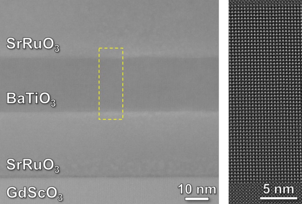
Seeking to harness these properties for use in microchips, the Berkeley Lab-led team developed a pathway for creating films of BaTiO3 just 25 nanometers thin—less than a thousandth of a human hair’s width—whose orientation of charged atoms, or polarization, switches as quickly and efficiently as in the bulk version.
“We’ve known about BaTiO3 for the better part of a century and we’ve known how to make thin films of this material for over 40 years. But until now, nobody could make a film that could get close to the structure or performance that could be achieved in bulk,” said Lane Martin, a faculty scientist in the Materials Sciences Division (MSD) at Berkeley Lab and professor of materials science and engineering at UC Berkeley who led the work.
Historically, synthesis attempts have resulted in films that contain higher concentrations of “defects”—points where the structure differs from an idealized version of the material—as compared to bulk versions. Such a high concentration of defects negatively impacts the performance of thin films. Martin and colleagues developed an approach to growing the films that limits those defects. The findings were published in the journal Nature Materials.
To understand what it takes to produce the best, low-defect BaTiO3 thin films, the researchers turned to a process called pulsed-laser deposition. Firing a powerful beam of an ultravioletlaser light onto a ceramic target of BaTiO3 causes the material to transform into a plasma, which then transmits atoms from the target onto a surface to grow the film. “It’s a versatile tool where we can tweak a lot of knobs in the film’s growth and see which are most important for controlling the properties,” said Martin.
Martin and his colleagues showed that their method could achieve precise control over the deposited film’s structure, chemistry, thickness, and interfaces with metal electrodes. By chopping each deposited sample in half and looking at its structure atom by atom using tools at the National Center for Electron Microscopy at Berkeley Lab’s Molecular Foundry, the researchers revealed a version that precisely mimicked an extremely thin slice of the bulk.
“It’s fun to think that we can take these classic materials that we thought we knew everything about, and flip them on their head with new approaches to making and characterizing them,” said Martin.
Finally, by placing a film of BaTiO3 in between two metal layers, Martin and his team created tiny capacitors—the electronic components that rapidly store and release energy in a circuit. Applying voltages of 100 mV or less and measuring the current that emerges showed that the film’s polarization switched within two billionths of a second and could potentially be faster—competitive with what it takes for today’s computers to access memory or perform calculations.
The work follows the bigger goal of creating materials with small switching voltages, and examining how interfaces with the metal components necessary for devices impact such materials. “This is a good early victory in our pursuit of low-power electronics that go beyond what is possible with silicon-based electronics today,” said Martin.
“Unlike our new devices, the capacitors used in chips today don’t hold their data unless you keep applying a voltage,” said Martin. And current technologies generally work at 500 to 600 mV, while a thin film version could work at 50 to 100 mV or less. Together, these measurements demonstrate a successful optimization of voltage and polarization robustness—which tend to be a trade-off, especially in thin materials.
Next, the team plans to shrink the material down even thinner to make it compatible with real devices in computers and study how it behaves at those tiny dimensions. At the same time, they will work with collaborators at companies such as Intel Corp. to test the feasibility in first-generation electronic devices. “If you could make each logic operation in a computer a million times more efficient, think how much energy you save. That’s why we’re doing this,” said Martin.